Minimizing costs are a key part of the semiconductor manufacturing process. Test is no exception, although steady improvements in efficiencies over the last 15 years have lowered the typical cost of test as a percentage of IC revenue to less than 2-3%. The primary drivers of increased efficiency have been reductions in capital costs per resource and test times , coupled with increases in parallelism and Built-In Self Test (BIST) capability. Most SOC device are tested 2 to 16 at a time, and memory devices can have in excess of 1,000 devices tested at once. Measured as the cost to use capital equipment for test (in terms of cost per hour per device), these decreases in test cost will continue at a relatively consistent rate per year. The figure below shows the historical rate of capital investment in test, interface (consumables) and handling equipment.

Figure TST1 – Test Costs as a percentage of device ASP (Used by permission of VLSI Research)
Looking forward, there are several trends which will counterbalance equipment efficiency and serve to cause cost increases:
Increases in transistor count that outstrips compression technology will increase the amount of external data which must be supplied to the Device Under Test (DUT). Coupled with scan shift rates that are limited by power and thermal concerns, the overall effect will be longer test times. This will be addressed primarily with increased parallelism
Device configuration and one-time programming during test is causing more time to be spent during test to perform initial device calibrations or to reconfigure devices based on defects or electrical performance. As silicon geometries shrink and defect densities drive circuit redundancy, repair functions will also add to test costs.
The eventual drive to multi-die packages will add a requirement for more System Level (“mission mode”) testing owing to lack of access to individual die. Without significant Design For Test (DFT) improvements, this type of testing can take much longer than conventional structural test. This will also drive more exhaustive test processes at wafer probe in order to improve the yield of multi-die packages
Even though continuous improvement in equipment efficiency will be offset by new device test requirements, the overall cost of test will continue to decrease. The major contributors to that cost are described in section 4.2
1.1 Cost of Test As a Part of Overall Manufacturing Cost[]
While the cost to own and operate test equipment has been reducing, other semiconductor manufacturing costs have been significantly increasing with new silicon technology. Specifically fab costs for leading-edge processes have increased to about 70-80% of the overall cost of producing a large-scale SOC device.
It now costs far more to fab a device than to test it, and that trend will accelerate as new fabrication technologies are deployed..
The figure below represents third-party analysis of the capital and service costs of equipment used in device fabrication, packaging and test.

Figure TST2 – Relative cost of Fab, Packaging and Test Equipment
While it is helpful to focus on the cost of test itself, the overall contribution to a manufacturer’s profitability from lower test costs will be very small since test is a small part of the device cost overall. The highest avoidable costs in test are devices that are good but are rejected at test for some reason.
Consider the following, simplified example.
· A device costs $1.00 to manufacture, including Fabrication, packaging, etc.
· Test constitutes 5% of that cost, or $0.05
Reducing the cost of test by 10%, will reduce overall costs by $0.05 X 10% = $0.005 per device
Improving yield by 1% reduces overall cost by $1.00 * 1% = $0.01 per device
While the 10% Cost of Test reduction is good, the yield improvement is better.
The figure below shows the effect on cost of test of traditional cost reduction techniques:


Figure TST3 – Cost of Test Reduction realized by traditional cost reduction techniques
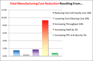
If one considers the effect on total manufacturing costs, including the cost to scrap devices that are actually good, the cost saving due to improved yield becomes far more significant.
Figure TST4 – Total Cost of Manufacturing Reduction realized by traditional cost reduction techniques

The risk of yield loss is increasing over time for several reasons:
· Trends such as the reduction of power supply voltages and more complex RF modulation standards will drive higher accuracy requirements for test equipment. Test equipment accuracy is typically added as a “guardband” in testing, reducing the range of acceptable measurements. If measured DC and AC values become smaller and there is no improvement in test accuracy, this guardband will cause more marginal (but good) devices to be scrapped.
· As noted earlier, many devices, especially for mobile applications require some sort of calibration or trim during the test process to improve DC and AC accuracy. This dramatically increases both the number of measurements made and the accuracy required of the test equipment. The requirements increase the chance of discarding devices that would otherwise have been good.
· Faster production ramps and short IC product life cycles will reduce the amount of time available to optimize measurements for the majority of devices produced
The remainder of this chapter will examine Costs associated with owning and operating test equipment. It must be stressed that reducing these costs must be done in the context of the overall cost to produce devices and balance reduction in test costs with potential reductions in product yield.
1.2 Test Cost Models and Cost Improvement Techniques[]


The cost of semiconductor test has many drivers as shown in which is further complicated for multi-die SiP precuts as shown in Figure TST5.
Figure TST 5 – Multi-die Flow
1.2.1 Current Top Cost Drivers[]
The traditional drivers of Test Costs typically include (In rough order of impact to Cost)
· Device Yield
· Test Time, site count and Parallel Test Efficiency (PTE)
· Overall Equipment Utilization
· ATE Capital & Interface Expenditures
· Facility/Labor costs
· Cost of Test Program Development
· Cost of die space used for Test-only functions
1.2.2 Future Cost Drivers[]
· Increased test time due to larger scan patterns
· Increased testing at wafer to produce Known Good Die (KGD)
· Addition of system-level testing
· Increased cost of handling equipment to support high site count or singulated die
· Increasing use of device calibration/trimming at test or device repair with redundant components
1.2.3 Currently Deployed Cost Reduction Techniques[]
· Multi-site & reduced pin-count
· Structural Test & Scan
· Compression/BIST/DFT and BOST
· Yield Learning & Adaptive Test
· Concurrent Test
· Wafer-level at-speed testing
1.2.4 Cost Reduction techniques that may be Deployed in the Future[]
· Advanced embedded instruments
· New contacting technologies
· In-system level testing to detect latent defects and potentially repair
· Built in fault-tolerance
1.3 Interface Cost Trend[]
Controlling the interface cost is essential for successful cost scaling using multi-site test: A dominating interface cost that increases exponential with the number of sites may defeat the purpose of increasing the number of sites. The interface cost becomes very challenging with high bandwidth (2 Gbit/s) and/or high multi-sites (128 sites). There is a need to develop consistent cost models that cover the wide range of probe card technologies in the market place. Long probe card lead times cause significant cost problems, especially for the advanced technologies.


Figure TST6 below shows the relative cost of Test equipment, handling equipment and interface material (consumables) in an SOC test cell
Figure TST6 – Distribution of costs in an average Test Cell
1.4 Multi-site Trend[]
As discussed in the previous sections, the most important way to reduce cost of test is increasing the number of sites. The effectiveness of increasing the number of sites is limited by (1) a high interface cost, (2) a high channel and/or power cost, and (3) a low multi-site efficiency M:
Where N is the number of devices tested in parallel (N>1), T1 is the test-time for testing one device, and TN is the test time for testing N devices in parallel. For example, a device with a test time T1 of 10 seconds tested using N=32 sites in TN =16 seconds has a multi-site efficiency of 98.06%. Hence, for each additional device tested in parallel there is an overhead of (1-M) = 1.94%.
Typical site counts for various device types are shown in Spreadsheet Table TST2.
  Figure TST7 – Importance of Multi-Site Efficiency in Massive Parallel Test |
As one continues to increase the number of sites, a low multi-site efficiency has a larger impact on the cost of test. For example, 98% efficiency is adequate for testing two and four sites. However, much higher efficiency is needed for testing 32 sites. At 98% efficiency going from testing a single site to testing four sites will increase a 10s test time to 10.8s. However, going from testing a single site to testing 32 sites will increase a 10s test time to 16.4s, that is, significantly reducing the potential advantage of multi-site. There are more efficient ways to reduce overall cost of test than going to the next setup with more sites in certain cases. Especially for high mix, low volume applications, there are many tester utilization challenges. In these setups, frequently, lower degrees of multi-site is preferable because test time improvement of techniques to improve utilization have a higher impact on the overall cost of test